Contact us to discuss Boundary Scan Tools and Services
Thank you for taking the time to read this Boundary Scan Tutorial.
If you have questions, or would like information on our Boundary SCAN products, please feel free to contact us on: 1-800-928-6038 or click the button to send us a note.
Welcome
This article is an overview of Boundary Scan technology and related applications.
eToolsmiths also hosts monthly in-depth webinars about Boundary Scan and other test related topics.
Please visit out webinar page for the latest information.
Boundary Scan Background
Let’s begin with a bit of history on why Boundary Scan came about.
Back in the late 80s and early 90s, several developments in circuit board technology came together to make board test more difficult, namely:
· The move to surface mounted devices
· The use of multilayer circuit boards
· The miniaturization of electronic products
· The lack of test points on circuit boards, due to these issues
As a result of these changes, traditional in-circuit test (ICT) tools, so-called bed of nails testers were no longer able to fully test Printed circuit boards (PCBs). To address this vexing problem, a consortium of companies–known as the Joint Test Access Group or JTAG.
NB: The JTAG group was originally know as JETAG (Joint European Test Access Group) since it members were European companies when it was formed was formed. The name was changed to JTAG shortly after inception when US and Asian companies joined the effort.
After the ratification of the core boundary scan specification known as IEEE1149.1, companies continued to advance the technology by proposing enhancements. The suggestions led to new versions and new standards that helped to keep pace with advancing IC and board technology. The major standards are outlined below and will be covered in more detail in this tutorial.
IEEE Standards
IEEE 1149.1 JTAG
IEEE 1149.1 standard describes the core functionality for JTAG Boundary Scan as it applies to digital circuit testing this tutorial will describe the standard in detail. The .1 spec supports static digital testing via Boundary Scan.
IEEE 1149.6 JTAG
Eleven forty-nine dot six adds support AC coupled nodes like LVDS.
It allows you to test by sending pulses back and forth between devices using cells that support LVDS signals.
In order to do this sort of testing you are required to have a cell with dot six support at each end of the bus.
IEEE 1149.7 JTAG
IEEE 1149.7 is a super-set of IEEE 1149.1 It provides increased capability and decreases the pin count on the TAP controller from five pins down to two. (1149.7 only requires the TMS and TCK signals)
This scheme reduces the number of pins needed on the IC for control and test. For fast, direct access to devices 1149.7 supports a star configuration.
See the video for additional detail on the 1149.1, 1149.6 and the 1149.7 specifications.
Obtaining the IEEE Standard
The IEEE 1149.1 Standard JTAG specification is available directly from IEEE: http://standards.ieee.org/
Who uses Boundary Scan?
Design Engineers
Design engineers use Boundary Scan for hardware bring up, validation and prototype debug. They may also use the tools to create tests for use in manufacturing.
Test Engineers
Test Engineers use Boundary Scan to creating tests for manufacturing and board repair.
Production Staff
Manufacturing staff use Boundary Scan tools to test and debug circuit boards in a production environment,
JTAG Boundary Scan Tools
The term JTAG is used loosely to describe board test and embedded debug interfaces based on the 1149.X specification. Terms typically used include:
Production test tools
Manufacturing staff use JTAG Boundary Scan tools to test and debug circuit boards in a production environment, using boundary Scan test vectors.
JTAG ICE Debuggers
The same JTAG interface that is used for Boundary Scan test can also be used by tools that enable debugging of embedded firmware on microprocessors and microcontrollers.
JTAG Device Programmers
Many popular programmable devices use the JTAG interface as well. to program devices in-circuit.
Contact us to discuss Boundary Scan Tools and Services
Thank you for taking the time to read this Boundary Scan Tutorial.
If you have questions, or would like information on our Boundary SCAN products, please feel free to contact us on: 1-800-928-6038 or click the button to send us a note.
Applications of Boundary SCAN
Boundary SCAN supports chip, board and system level tests. This section introduces the types of tests possible with Boundary SCAN.
Prototype Debug and Bring Up
When bringing up and debugging your new hardware, Boundary Scan comes to the rescue in several important ways:
Testing Partially Populated hardware
When you get your initial boards, not all devices may be fitted. That’s fine, with Boundary Scan, you only need good power, ground and at least one part on the JTAG Chain to begin testing. You should be able to ID the part on the chain and then test for opens and shorts for any board area that is touched by this device.
Initializing and Programming Devices
You may also be able to do initial device programming. For example, if the device on the chain is a microprocessor or DSP, most likely you will have access to RAM and FLASH memory via the address, data and control bus. This can allow you to ID and Program and test these so-called (cluster, or non-jtag) devices. FPGAs, CPLDs (XILINX and ALTERA, for example) may also fall into this category.
Finding Assembly Defects
Prototypes are often rushed through assembly in order to make engineering deadlines. As a result, assembly and manufacturing problems will exist. Boundary Scan is perfect for testing for common problems like unfitted or ill fitted devices, solder issues (cold or hot Joints), as well as open, shorts, stuck at and device functional failures.
Hardware Validation
As initial firmware or diagnostics are written for your new hardware, Boundary Scan can be used to rule out “bad hardware” by providing a “golden” test that validates that a board is good. With this type of testing, you will be able to focus your debug efforts on the new release of firmware, knowing full well that your hardware is good.
Production Test
Manufacturing test is the clearly sweet spot for Boundary Scan. It was designed to complement existing test methods and to overcome the problems of evolving board technology.
Device Programming
As previously mentioned devices can be programmed via JTAG boundary Scan. CPLD and FPGA images can be loaded as well as boot loader code and diagnostics software. Boundary Scan also makes a perfect tool for production test repair stations that allow test engineers to troubleshoot complex and expensive boards in the “bone yard”.
Functional Testing
JTAG can be used to do basic functional testing of your hardware, including DDR RAM, FLASH, I2C based devices and others. Since JTAG is a clocked serial interface, some devices will be too fast to be tested at full speed but can be tested for general operation.
Processor-Controlled JTAG Test
Processor controlled test uses the same JTAG hardware interface and protocol as Boundary Scan testing, the difference is that the microprocessor on the board under test is used to implement the tests. Processor controlled test supports access to devices not accessible to JTAG and also supports “at-speed” testing.
Boundary SCAN Theory of Operation
The process of boundary scan can be most easily understood with reference to the schematic diagram shown in figure 1.
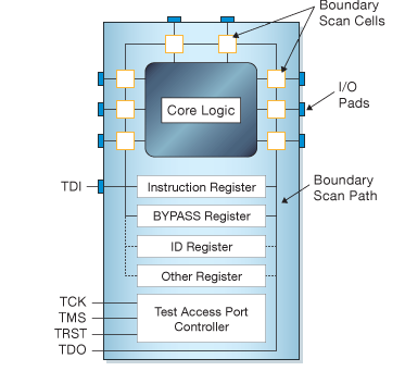
Signals between the device's core logic and the 'pins' are intercepted by a serial scan path known as the Boundary Scan Register (BSR).In normal operation these boundary scan cells are invisible. However, in test mode the cells can be used to set and/or read values: in external mode these will be the values of the 'pins'; in 'internal' mode these will the values of the core logic.
Interface Signals
The JTAG interface, known as a Test Access Port, or TAP, uses the following signals to support the operation of boundary scan.
TCK – 'test clock' synchronizes the internal state machine operations
TMS – 'test mode state' is sampled at the rising edge of TCK to determine the next state.
TDI – 'test data in' represents the data shifted into the device's test or programming logic. It is sampled at the rising edge of TCK when the internal state machine is in the correct state.
TDO – 'test data out' represents the data shifted out of the device's test or programming logic and is valid on the falling edge of TCK when the internal state machine is in the correct state.
TRST – 'test reset' is an optional pin which, when available, can reset the TAP controller's state machine.
| Figure 1 - Schematic Diagram of a JTAG enabled device |
Registers
There are two types of registers associated with boundary scan. Each compliant device has one instruction register and two or more data registers.
· Instruction Register – the instruction register holds the current instruction. Its content is used by the TAP controller to decide what to do with signals that are received. Most commonly, the content of the instruction register will define to which of the data registers signals should be passed.
· Data Registers – there are three primary data registers, the Boundary Scan Register (BSR), the BYPASS register and the IDCODES register. Other data registers may be present, but they are not required as part of the JTAG standard.
· BSR this is the main testing data register. It is used to move data to and from the I/O pins of a device.
· BYPASS – this is a single-bit register that passes information from TDI to TDO. It allows other devices in a circuit to be tested with minimal overhead.
· IDCODES – this register contains the ID code and revision number for the device. This information allows the device to be linked to its Boundary Scan Description Language (BSDL) file. The file contains details of the Boundary Scan configuration for the device.
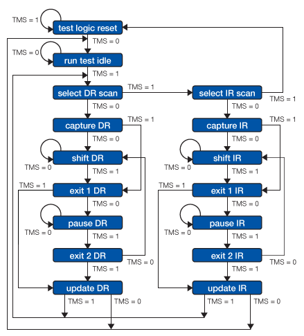
Test Access Port (TAP) Controller
The TAP controller, a state machine whose transitions are controlled by the TMS signal, controls the behavior of the JTAG system. Figure 2, below, shows the state-transition diagram.
All states have two exits, so all transitions can be controlled by the single TMS signal sampled on TCK. The two main paths allow for setting or retrieving information from either a data register or the instruction register of the device. The data register operated on (e.g. BSR, IDCODES, BYPASS) depends on the value loaded into the instruction register.
For more detail on each state, refer to the IEEE 1149.1 Standard JTAG document.
| Figure 2 - TAP State machine |
Boundary Scan Instructions
The IEEE 1149.1 standard defines a set of instructions that must be available for a device to be considered compliant. These instructions are:
BYPASS – the BYPASS instruction causes the TDI and TDO lines to be connected via a single-bit pass-through register (the BYPASS register). This instruction allows the testing of other devices in the JTAG chain without any unnecessary overhead.
EXTEST – the EXTEST instruction causes the TDI and TDO to be connected to the Boundary Scan Register (BSR). The device's pin states are sampled with the 'capture dr' JTAG state and new values are shifted into the BSR with the 'shift dr' state; these values are then applied to the pins of the device using the 'update dr' state.
SAMPLE/PRELOAD – the SAMPLE/PRELOAD instruction causes the TDI and TDO to be connected to the BSR. However, the device is left in its normal functional mode. During this instruction, the BSR can be accessed by a data scan operation to take a sample of the functional data entering and leaving the device. The instruction is also used to preload test data into the BSR prior to loading an EXTEST instruction.
Other commonly available instructions include:
IDCODE – the IDCODE instruction causes the TDI and TDO to be connected to the IDCODE register.
INTEST – the INTEST instruction causes the TDI and TDO lines to be connected to the Boundary Scan Register (BSR). While the EXTEST instruction allows the user to set and read pin states, the INTEST instruction relates to the core-logic signals of a device.
BSDL Files
Boundary Scan Description Language (BSDL) is a subset of VHDL that is used to describe how JTAG (IEEE 1149.1) is implemented in a particular device. For a device to be JTAG compliant, it must have an associated BSDL file.
These files are often available for download from manufacturers' websites.
JTAG systems such as XJTAG use the information contained in a BSDL file to work out how to access a device in the JTAG chain.
BSDL files contain the following elements:
· Entity Description: Statements naming the device or a section of its functionality.
· Generic Parameter: A value such as a package type. The value may come from outside the current entity.
· Port Description: Describes the nature of the pins on the device (input, output, bidirectional, linkage).
· Use Statements: References external definitions (such as IEEE 1149.1).
· Pin Mapping(s): Maps logical signals in the device to physical pins.
· Scan Port Identification: Defines the pins used on the device to access the JTAG capabilities (TDI, TDO, etc - the Test Access Port).
· Instruction Register Description: The signals used for accessing JTAG device modes.
· Register Access Description: Which register is placed between TDI and TDO for each JTAG instruction.
· Boundary Register Description: List of the boundary scan cells and their functionality.
Testing non-JTAG Devices
Including tests for devices that do not have JTAG is very important in achieving the highest possible test coverage. Connection testing is very good at checking the physical, manufacturing integrity of a lot of a circuit; however there are faults that it cannot detect. For example it is only possible for a connection test to check that a pin is not open circuit if communication can be seen between that pin and another pin in the design. This means that a connection test can only check for open circuit faults on pins that have JTAG capability and are on nets with at least one other JTAG enabled pin.
However, by using the connections between the accessible pins/busses on devices in the JTAG chain to drive and monitor signals on non-JTAG devices, it is possible to test other pins for open circuit faults. Exercising the functionality of non-JTAG devices in this way means that open circuit faults can be found on both the peripheral device and the JTAG enabled device.
Short circuit faults and stuck-at faults can also be detected in this way; however connection testing is a more effective tool for finding these types of fault.
This form of testing can be used on individual devices but is often applied to a group, or cluster, of non-JTAG devices in the circuit. Some JTAG tool vendors refer to this type of testing as cluster testing.
Memory Testing
One variant of this method is memory testing. A sequence of JTAG test signals is created to manipulate the address and data busses of a memory device so as to write information into memory, then a second set of test signals is created to read this information back. This can apply to SRAM, SDRAM, Flash memory or any variant.
Other Possibilities
If any non-JTAG device is connected to a JTAG device, its functionality and/or connections can be tested to some extent. For instance:
· External Connectors
· Video chips
· IIC devices
· Ethernet Controllers
· LEDs
· Switches
· and many more..
Find out More
Thank you for taking the time to read this article. If you have questions, or would like information on our Boundary SCAN products, please feel free to contact us on: 1-800-928-6038 or Contact us.