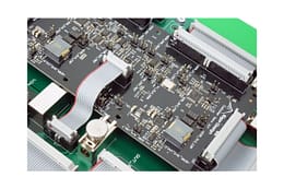
Prototype Printed Circuit Board Test
Prototype Printed Circuit Boards are early versions of electronic circuits. The first revisions of these boards usually have errors and require debug and test.
Electronic product manufacturers (OEMs) typically send the files produced by their schematic capture package to a circuit board FAB or Prototype house for to be built.
Often so-called quick turn PCB Fab houses are used to quickly deliver the first versions of the circuit board to help meet tight deadlines.
When the new boards arrive, hardware engineers must verify that the first prototypes work as expected. A brief description of prototype debug is detailed below.
Review Test Reports from the CM
Depending on a boards cost and quality, the OEM can to equip their CM with test equipment for the first run of hardware.
Optionally, CMs may develop test fixtures and tests for the OEM under contract. In each case, new boards are tested, then sent to the OEM along with a test report. Before bringing up the board for the first time, engineers can consult these reports to see if there are any problems with the board. Based on the report, the engineer will correct problems found before powering up the system.
Perform Visual Inspection
New prototypes are often inspected to verify all components are correctly fitted and that there are no obvious errors.
First Prototype Power-up
Next an Engineer will apply Power to the board for the first time. Often called the "smoke test", because if there is a serious problems there may actually be smoke as components fail!
JTAG Boundary SCAN Test and Debug
IEEE 1149.1 JTAG Boundary SCAN test is typically used to debug complex hardware designs, especially if the designs lack test points an/or have surface mount devices. JTAG Boundary SCAN is great since it leverages the chips on the board to test the circuit.
To support the JTAG "pins out" test method, the prototype must include at least on device that supports IEEE 1149.1 and also provide access to the device via the JTAG pins: (TDI, TDO, TMS, TCLK and optionally TRST). JTAG Test tools also need a boundary scan description language file or BSDL file that describes how IEEE 1149.1 is implemented on the device along with a net list file describing device connections for the circuit.
Boundary SCAN can:
- Program and Configure devices such as: FPGAs, CPLDs, FLASH, etc.
- Test for open shorts and stuck at failures
- Functionally test devices like RAM, FLASH, Ethernet etc.
Functional Test
Functional tests in addition to those supported by Boundary SCAN can also be run on the board. These tests are typically used to test the system "at speed" which in some cases will be difficult to do with Boundary SCAN. Functional tests work by loading and running code on a microprocessor in the system. The code can be loaded by a JTAG Tool if required.
Re-spin and repeat until release
Based on the number and type of errors found with the prototype board, a re-spin of the board could be needed. The re-spin will include changes to the circuit design and layout to address any issues found during prototype testing. The board is then created by the fabrication house and the test process repeats until the board is ready to ship.
Full Production tests for manufacturing
Once the board ready for volume manufacturing, engineers create a test strategy for the board. Test methods include, but are not limited to:
- In-circuit Test (ICT)
- JTAG Boundary SCAN test
- Functional test
- XRAY and Optical inspection

